
KiCad: Edge cut and copper zone from CAD sketch
Created: 2024-06-24
Limitations in physical space..
..or why weirdly shaped PCBs exists. When creating edge cuts for my PCBs I find that the built-in KiCad PCB editor tools to be limited. Sure you can draw lines, arcs, rectangles and circles, which is fine for most simple PCB shapes but for more complicated shapes it's not something I would rely on entirely. Even if I manage to create the shape I want, I still need to find a way to incorporate it into a CAD program to design an enclosure for it. There are ways of exporting KiCad edge cuts into file formats that can then be parsed in other CAD programs. That workflow is flawed when starting with a finished enclosure or specific limitations in dimensions for the PCB. When the PCB needs to adapt to some other shape. Enter DXF graphics support in KiCad!
Disclaimer: I'm not sure when this feature added to KiCad but I know for sure that this works for KiCad 8+
DXF and Onshape
DXF (or Autocad DXF) is a file format developed by Autodesk for enabling interoperability between CAD programs. Onshape is a web based 3D CAD application that I primarily use as an alternative to Autodesk Fusion. I do that simply because there is a free plan that is reasonable for non-commercial use. One of the features that Onshape supports is exporting 2D sketches of what you make e.g. for a weirdly shaped object you draw you can export the projection of the object as an exported DXF file. This file can then be imported into KiCad.
Edge cut from DXF
First a sketch needs to be made from a CAD program that supports DXF export.
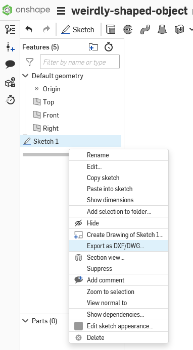 This example uses Onshape. Press the green button to finish sketch. The DXF can then be exported by right-clicking the sketch and pressing "Export to DXF/DWG"
 Open the PCB editor in KiCad and go to
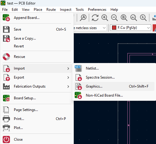
 File > Import > Graphics (or if you are a cool shortcut kiddo press Ctrl + Shift + F)
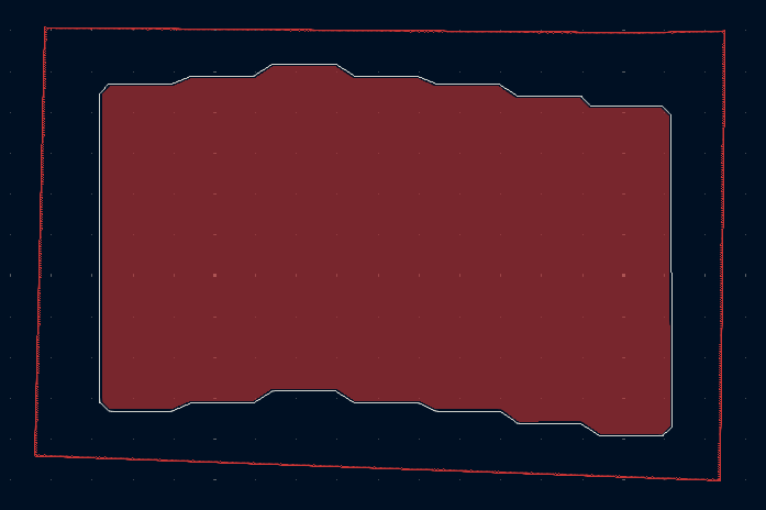
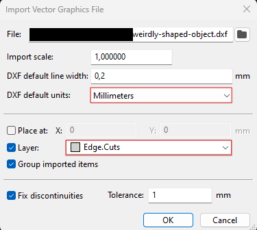 A prompt will appear. Select the correct units that you used in your CAD program when exporting the DXF. I use millimeters in both Onshape and KiCad (it does not make sense to mix units.. between CAD programs). Then select "Edge.Cuts" as layer, press OK.
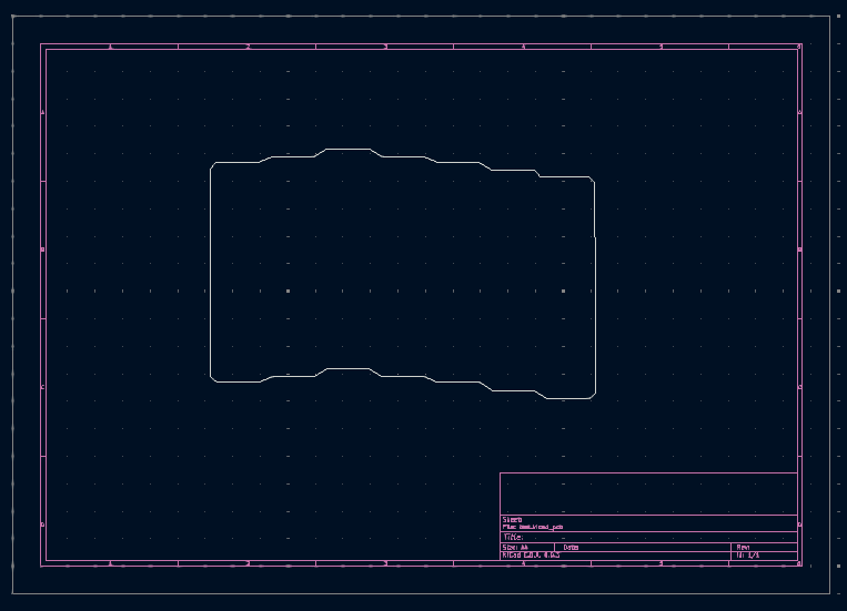 The results should look like this if you use the default colorscheme in the PCB editor. White lines are the color of "Edge.Cuts" layer.
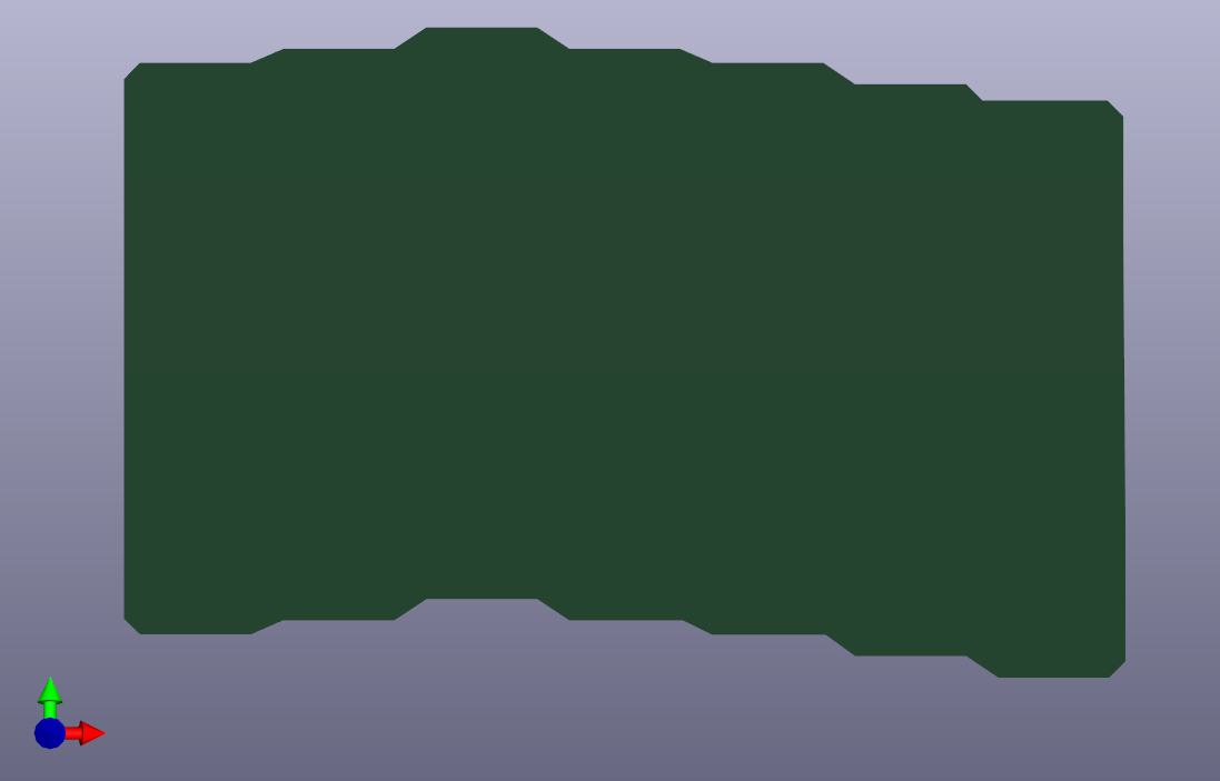 ..and the 3D model should show you that the edge cut is parsed correctly. Another disclaimer is that maybe not every manufacturer is able to do very complex shapes. Make sure you check this with the manufacturer guidelines before ordering something strange.
Copper zone from DXF
In normal cases when I make a copper zone for GND or for VCC I select the Add Filled Zone tool (Ctrl + Shift + Z), make a big square that covers the whole PCB then press B to fill all zones and it works just fine.
 It looks like this.
But what if you want the filled zone borders to look more tidy? There is a way to import DXF and then convert its shape into a filled zone. It looks cleaner but other than that there are are not many benefits of doing this.
- Follow instructions on how to import DXF as an edge cut.
- Set active appearance layer to F.Cu.
Right-click > Enter group > Right-click > Create from selection > Create zone from Selection, Add Filled Zone prompt should appear- Un-tick "Delete source objects after conversion". Else edge cut needs to be re-added once ok is pressed. (If the shape is too complex the layer KiCad will not add a filled zone and nothing will happen)
- Press B to fill zones.
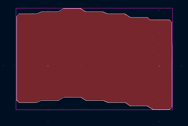 .. and now the edges of the filled zone matches with the edge cut that comes from the DXF.
This DXF is actually from a keyboard PCB I'm working on where I derive the copper zone from the DXF and uses it to guide a via stitching addon to follow its edge. An upcoming post will show how that is setup.